
thermoelectrics: was that Intel as the assignee?
I last posted an
article about thermoelectrics in January 2008. These materials continue to be an area of great interest, as the technologies develop and their utility is further demonstrated. This recent abstract from Nature discussing advances in superlattice-based structures is a case in point. It is worth noting that several co-authors are from Intel. This is no surprise as the semiconductor industry has always been considered a prime market for superlattice-based thermoelectric structures because of the industry’s great experience with deposition techniques and equipment that is applicable to superlattice structure fabrication.
The author list reminded me of United States patent 7,279,796 (the ‘796 patent) to Hu, Chrysler and Mahajan, and assigned to Intel. This patent details a basic structure for adding a thermoelectric device to an integrated circuit.
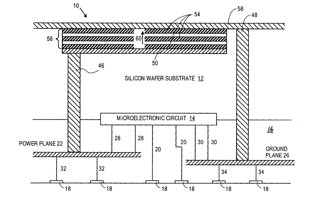
With reference to the above representative figure from the ‘796 patent the integrated circuit 14 is located on one side (bottom here) of silicon wafer 12, while thermoelectric module 56 is located on the other side. Metal vias 46 and 48 then connect module 56 to the power and ground planes, within the metallization 16, respectively.
Thermoelectrics have always presented a compelling story and promise. Their application to integrated circuits is particularly interesting because they are solid state, an ICs thermal loads are reasonable and their fabrication may well be compatible with semiconductor processing. Any successful system could provide competitive advantages in either reducing the power consumed in mobile devices or reducing the energy expended cooling large installations. This goes hand-in-hand with the growing efforts to “green’ data centres and other IT infrastructure.