
thermoelectric materials – road to the solid state fridge
There is plenty of waste heat in society. In fact, it is difficult to think of a process that does not lose energy to heat. It might be an internal combustion engine, a light bulb, an electrical motor or an integrated circuit. They all produce unwanted heat. An often quoted number for the fraction of input energy that is lost to heat in a combustion process is 70%. To top it off, additional energy might be consumed to remove or “deal with” this heat.
Is there a way to recover this energy? Is there a way to convert this heat into a more useful form of energy. Thermoelectric materials come to mind. They can generate electricity directly from a temperature difference, as would be created by waste heat. A very nice aspect of thermoelectric materials is the absence of moving parts, allowing them to be applied to an exhaust pipe or the surface of a semiconductor. To date thermoelectrics have been used in niche applications, but commercial use is still elusive. Two hurdles to commercial use are low conversion efficiency and cost.
Thermoelectric materials generate an electrical current when there is a hot surface and a cold surface. They must provide good electrical conductivity and poor thermal conductivity, where the latter maintains the temperature difference between surfaces. This combination of conductivities is not normal. Consider copper as an example. It has both high electrical and thermal conductivity as one anticipates from a metal. It is a poor thermoelectric material because the high thermal conductivity mitigates the temperature difference. Generally, one needs to engineer or design a material to provide for these properties.
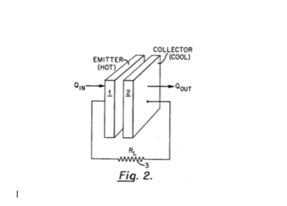
I will look at one old and one new thermoelectric. An older approach is the so-called Huffman junction. The concept of the Huffman junction was outlined in United States patent 3,169,200, which issued in 1965. As presented in Fig. 2, reproduced below, the thermoelectric device has two surfaces that are separated by a small space. A temperature difference between the two surfaces causes electrons tunnel across the space or “junction” with a net flow from the hot to the cold surface. Today work is continuing on both the structure and methods of fabrication. As might be anticipated it is no small task, no pun intended, to provide a space with the required dimensions.
A newer approach uses superlattice structures i.e. stacks of thin layers of material. In one example, the active thermoelectric component is based on a superlattice of ~1 nm layers of alternating material. Structures implementing p-type Bi2Te3 & Sb2Te3 alloys (Venkatasubramanian R. et al. Thin-film thermoelectric devices with high room-temperature figures of merit. Nature 413, 597 (2001)) have demonstrated improved thermoelectric properties. A structure based on such a superlattice active is detailed in United States patent 6,300,150, for example.
With rising energy costs and advances in manufacturing techniques thermoelectric systems will continue towards commercialization. However, there is plenty of work to be done. The first commercial applications may include integrated circuits and other electronic systems. Once systems can be scaled to larger amounts of heat thermoelectrics might be targeted at refrigeration and general cooling markets. The payoff for a system that can generate electricity from waste heat is too large to ignore.