
crystal solar … beep … beep … beep
OK a mid-September Technology Review
article on Crystal Solar was sitting on my desk for a bit. There were notes all over it correcting some dodgy statements about poly-silicon, but its essence had not jelled, there were just too many dangling bits. In the end there was only one thing to say; “let’s backup a bit”.
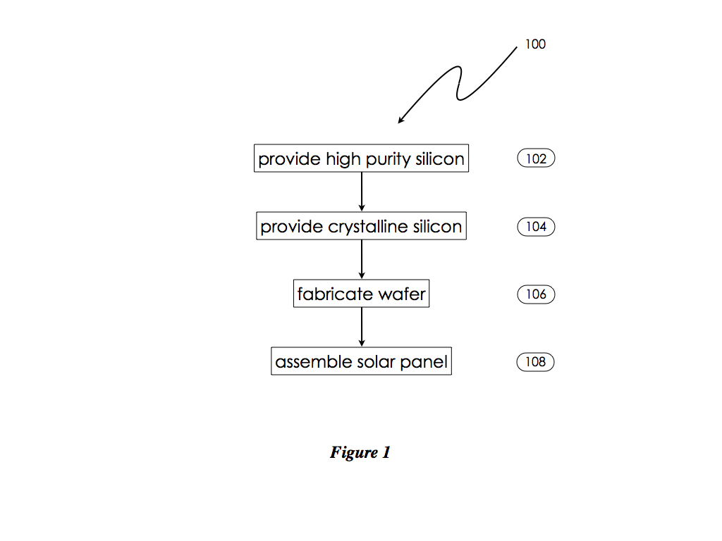
At its most basic the method of fabricating silicon based solar panels has four broad steps. A flow chart of this method 100 is presented in Figure 1. First, high purity silicon is provided at step 102. Crystalline silicon, either poly-crystalline or a single crystal, is then produced at step 104. Next, a silicon wafer is fabricated from the crystalline silicon at step 106. Finally, the wafer is used in the fabrication of a solar panel at step 108. That is it. There is of course further granularity and variation within each step, but everyone has to start with high purity silicon and end with a finished panel. The key to looking at a new entrant is seeing how it accomplishes this basic method and consider on which of these steps it has focused its research.
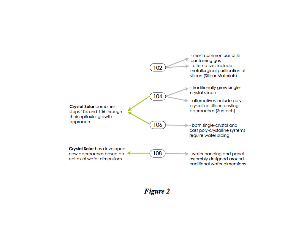
So where does Crystal Solar fit? To answer this it is worth looking at Figure 2, which pictorially illustrates how their approach fits into the basic steps of Figure 1. Figure 2 also presents some of the variations other companies have implemented. Crystal Solar’s technology is centered around the use of epitaxial growth to fabricate wafers. This approach combines steps 104 and 106 into a single step. As mentioned in a 2009 Technology Review article the use of epitaxial growth results in thin wafers or sheets which require the development of new systems for handling them at step 108.
Finally, it is worth taking a brief look at published US patent applications assigned to Crystal Solar. Looking at the titles of the eight applications, they confirm research and development around epitaxial growth, including the reactor, and systems and methods for assembling the wafer into panels. As usual with these articles one could take a much closer look at the technology, but that is for a different forum. At the moment I think it is helpful to slot the basic technology.