
Apple’s Growing Semiconductor Design Capabilities : the A8 and A8X
The Watch portion of Apple’s Spring Forward keynote was long on style, mid-distance on functionality and short on details around enabling technology. In particular, there were no details on the chips “driving” it.
Yes these are behind-the-scenes details, but the likely appearance of an IC from Apple would add another important piece in their overall semiconductor technology strategy puzzle. With the introduction of the 27” Retina iMac in the fall of 2014 Apple indicated that they designed their own display controller, because they could not find what they wanted. This little bit of information reiterates their semiconductor design capabilities. It also speaks to the apparent modus operandi for the semiconductor division; we can design what we need.
Will this apply to the Watch? Does it apply to their flagship A-series of processors? What did the A8 and A8X tell us about Apple’s design capabilities?
Last fall’s iPhone 6 and iPad Air 2 brought us the A8 and A8X iterations of the A-series family, respectively. Figure 1 presents die photographs of the A8(left) and A8X(right). The “X” side of the family returned after its absence in the “7” generation. As usual the media seemed to fixate on the identity of the foundry. With TSMC identified as the foundry for the A8 and A8X we witnessed the long rumoured move from Samsung. Also without deviating from the script, the media seemed to only consider the CPU and GPU when discussing the design of the A8/A8X. Do not get me wrong these are important bits. They are however not the only bits. In fact the “8” generation continues the trend of increasing complexity outside of the CPU and GPU. It is time then to look at some numbers, and compare them to previous generations.
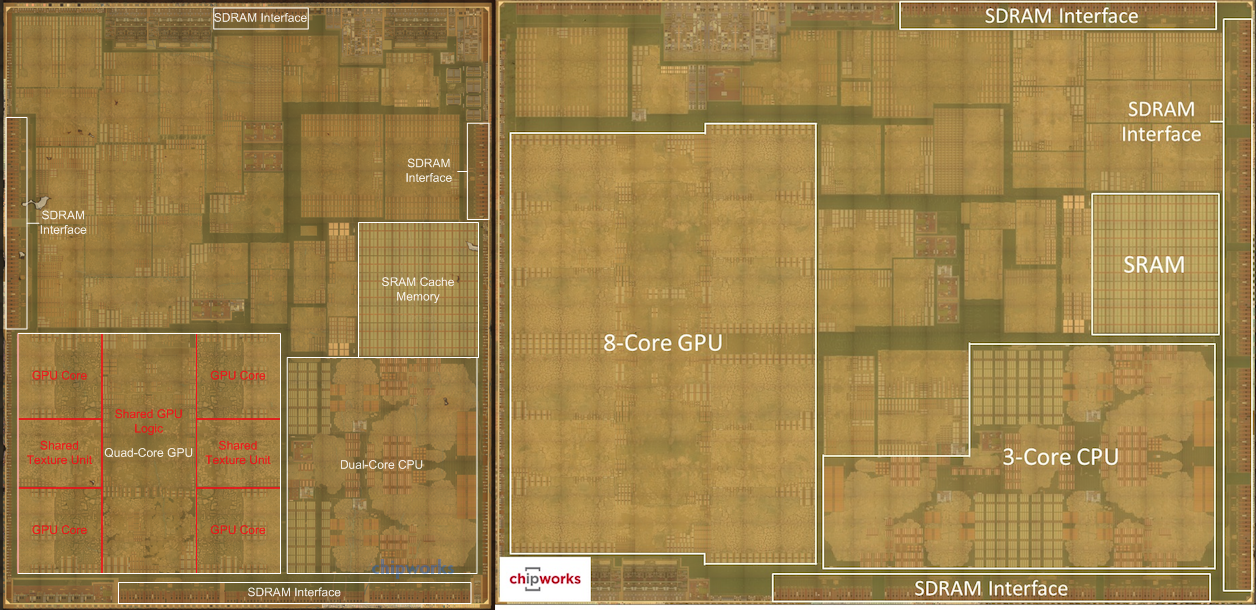
Source: Chipworks
by the numbers
Apple’s A-series family has seen a number of process iterations over its history. The A4 was fabricated with a 45 nm process while the A8/ A8X are fabricated with a 20 nm process. It is worth remembering that the “nm” number is the minimum feature size of that process. Thus the features of the A8 are less than half the size of those of the A4. So, when someone writes that the die size of the A8 is 87% that of say the A7 it is only “physically” true. Yes, the die size reflects the actual real estate of silicon and the cost of the die. It does not though accurately reflect the circuit design story. In order to get an understanding of this aspect one has to “normalize” die measurements to the same process geometry i.e. changes in die size reflect changes in the circuit design, not the process used for fabrication. From here one can more accurately compare the number or complexity of circuits, which reflects the functionality and computing capabilities or horsepower, if you will.
I have been tracking the normalized die size since the A6, or when the first move to a smaller process took place. Chipworks made a reference to the same calculation in their blog post on the A8. Before looking at numbers it is noted that I will look at the change in the overall die size, CPU, GPU and “other”, which has historically captured all circuitry outside of the CPU and GPU.
Onwards, Table 1 presents some key numbers for the A4 to A8 generations. This includes the actual, measured die sizes and those normalized to a 32 nm process. In terms of the A8 and A8X the numbers are quite astounding. As per the standard line the actual A8 die is slightly (13 %) smaller than the A7. However, if one looks at the normalized numbers the A8 comes in at 218 sq. mm compared to the A7’s 136 sq. mm. That is an additional 82 sq. mm or 60%. The normalized A8X die size comes in at 314 sq. mm, representing another 96 sq. mm beyond the A8 or 177 sq. mm larger than the A7. Another way, the A8X is 44% and 136% larger than the A8 and A7, respectively. So, in moving from the iPad Air to Air 2 the A-series processor more than doubles in size (design wise). That is impressive.
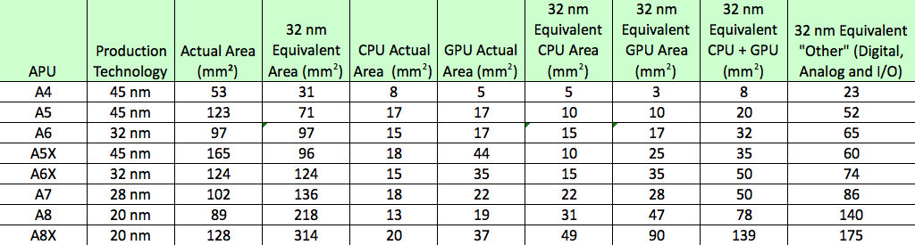
The standard line in articles that have been written to date is that the above differences can be attributed to the CPU and GPU, with the rest being “stuff” that makes the chip functional. Again, let’s take a look at the numbers. Is this what they tell us? The combined CPU and GPU (normalized) area increases by 28 sq. mm and 89 sq. mm from the A7 to the A8 and to the A8X, respectively. The “other blocks” area also increased by 89 sq. mm, from the A7 to the A8X. It is noted though that a large fraction of this “other blocks” increase (54 sq. mm) was between the A7 and A8, and a smaller amount (35 sq. mm) from the A8 to A8X. So, yes, there was a fair increase in the CPU + GPU area, particularly for the GPU of the A8X. However, there was an equally large increase in the “other ” circuitry. Further, this increase in “other” is not due to the large memory block that first appeared in the A7 and appears again in the A8/A8X.
We knew from Tim Cook’s fall Keynote that the A8X added quite a few circuits to come up to the claim of 3 billion transistors. This though did not seem to take hold as many pundits simply focused on the CPU and GPU. The simple analysis of areas presented above quantifies this increase in circuits. It also reiterates that there is plenty more to the A-series devices than the CPU and GPU. This of course leads us to design, design and design. Forget the discussion on foundry identity, Apple is focused on the design of their processors; design that will differentiate the end product from their competitors.